Understanding Transistor Circuits
07/16/2001
Introduction
During the many years of teaching transistors, transistor behavior, and transistor circuits.. it suddenly became obvious that the normally accepted sequence of teaching DC/AC/Solid State, was actually a very ineffective sequence. Anyone who has taught transistor theory, finds themselves having to review extensively all of the DC principles that a student was supposed to have down pat. However, being the normal human beings that we are, it seems that there is a great deal of "forgetfulness" that rears it's ugly head between DC and the completion of AC. It seems that most instructors seem to take it for granted that the student (having had a very firm grasp on those DC principles) is somehow fluent in all that has been taught before.... but not so for most of us! Having progressed through all of the complexities and nuances of reactance, phase angles, and all of the impedance considerations, surely the student remembers all that they were taught about DC. But, alas, this is not normally so. What I found was that if I taught transistor theory immediately after DC, the students were able to relate much more quickly to all of the transistor circuit concepts. The reason... simply because most of transistor theory is DC related! Also, as in many cases, a lot of the age-old "normal cookbook methods" are rather sterile in their method of presentation.
First Consideration:
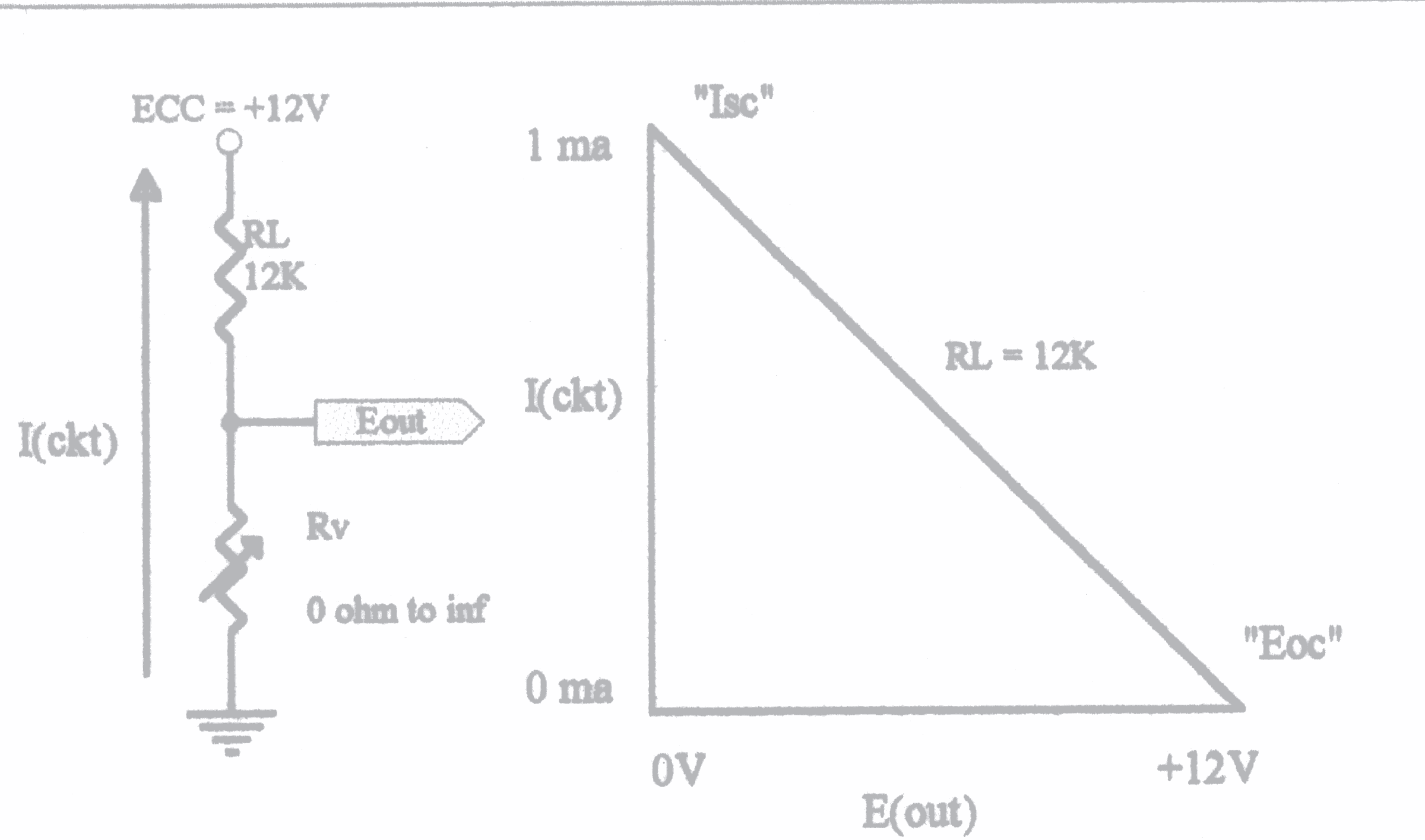
Place 2 resistors in series with each other between ground and a supply voltage of +12V. Now, consider that the resistor closest to the +12V is a fixed value of 12K. The resistor closest to ground we consider it as a variable that ranges between 0 ohms (dead short) and infinity ohms (open circuit). Now, compute the two extreme values of that circuit, first with the variable resistor shorted, and then the other extreme with the variable resistor open. For all practical purposes you will find about 1ma through the circuit with the variable resistor shorted. Now, imagine that the fixed resistor of 12K is like a spring tied to a recess in the ceiling, and the variable resistor is like a crowbar or lever of some sort that can pull the bottom of the spring to the floor. Now, it's easy to think of that situation, where the base of the spring can be simply pulled down to the floor, or let go, where it will rise to the top of the ceiling. This is what a transistor can do, as a variable resistor or conductor, where it simply pulls down the base of the fixed resistor to the "floor" (ground) or lets it go up to the top of the ceiling (+12V).
Second Consideration:
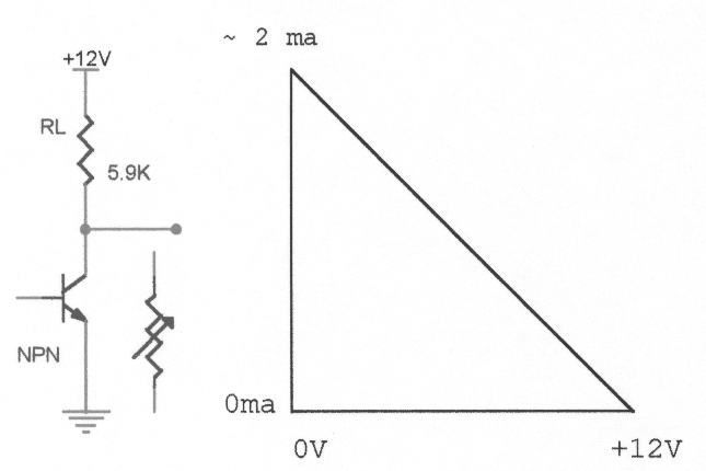
Now, here's the most important but simple part... If you simply plot the relationships of the voltage at the point between these 2 resistors (5.9K fixed) vs the current flow between them, you will get a straight line that goes directly from the +12V and 0ma at one end of the line to the 0V and 2ma at the other end of the line. This is simply where the variable resistor as a short circuit, will draw the base of the fixed resistor to ground, and cause about 2ma to flow in the series circuit. In the same manner, if the variable resistor is an open circuit, no current will flow, and the voltage at the base of the fixed resistor will be the supply voltage of +12V, because there is no voltage drop across that fixed resistor. These two basic concepts are of course obvious, but not everyone realizes that there can be drawn on a graph a straight line between these two points. Technical folks will tell you that since this is a straight line, that it represents a linear circuit. We need to also understand that it is the fixed resistor that causes this linear relationship, not the transistor!
Another important consideration is that these two extreme points have significant names! At the ground point of this straight line on our graph, that point is called "Isc", meaning "Short Circuit Current", or: "Current, of the Short Circuit variety". The point at the top of the straight line on our chart, is called "Eoc", meaning "Open Circuit Voltage", or: "Voltage, of the Open Circuit variety".
Third Consideration
We are going to replace that variable resistor with a variable resistive device, called a transistor (which means "transfer of resistance"). We should realize that where a transistor can be turned ON, or turned OFF, it does not do a perfect job of it. What happens is that when you try to turn a transistor off, it almost does, but there is a miniscule amount of current that quite literally "leaks" through, called interestingly enough "leakage current". When we try to turn on that same transistor to it's maximum capability, we find that it is not a perfect conductor, in that it exhibits a certain amount of small resistance, called "saturation resistance". First, this does not change our straight line on that graph. What it does show us though, is that there are limits to just how close we can come to those end points on that straight line. It is also very important to remember that as we gradually turn that transistor on, from an Off state, that those voltage/current relationships will stay right on that line! It will not fall outside or inside of that line, no matter what that transistor does in conduction!
Fourth Consideration
A special note: These two points are also significant, as they represent those two special identities known as "Norton's Equivalent Circuit Analysis" (which uses Isc), and "Thevenin's Equivalent Circuit Analysis" (which uses Eoc). These might seem to be too technical for the average person, but I strongly disagree. They are extremely beneficial tools, are certainly well worthwhile the effort to learn, and if approached correctly they are not bad at all (they only seem that way).
![]() Thevenin's Equivalent Circuit Analysis
Thevenin's Equivalent Circuit Analysis
![]() Norton's Equivalent Circuit Analysis
Norton's Equivalent Circuit Analysis
In both Vacuum Tube and Transistor considerations, there are 3 principle concepts that are quite valuable. They relate to what is called "Configurations", which is nothing more than how that respective device will behave in certain arrangements of signal inputs vs signal outputs and a common point between them. These are especially important considerations because they allow us to evaluate the performance of these devices as amplifiers and how they not only handle the loads attached to them, we can also evaluate how these devices affect their signal sources. The "common point" between the input and output signals involves the emitter as the "Common Emitter Configuration", the base as the "Common Base Configuration", or even the collector as the "Common Collector Configuration". Each of these configurations have advantages and disadvantages in their respective uses, as well as differences in their behaviour. The Common Collector Configuration is commonly known as the "Emitter-Follower" circuit. We need to remember that the bi-polar transistor is a current controlled device, in that whatever controls the base current controls the collector current, regardless of the type of configuration involved. The collector current is more than the base current by a ratio called the "Gain Factor", more simply called the "Beta" of the transistor.
We can take a look at each of these various (3) configurations one at a time or compare them against each other all at once by using printable PDF file. Realize also, that no matter what configuration we examine, the collector current is Beta times more than the base current. In my opinion, most of the books that present these configurations really unnecessarily confuse the issue about these current relationships. We'll discuss this more in detail later.
| NPN Common Emitter Configuration | NPN Common Base Configuration | NPN Common Collector Configuration |
| PNP Common Emitter Configuration | PNP Common Base Configuration | PNP Common Collector Configuration |
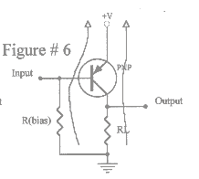
We can also look at a couple that look like Common Collector Configuration, but they're not! Remember that the true Common Collector Configuration is commonly referred to as an "Emitter Follower".
| Suprise #1 | Suprise #2 |
Always look for where the signal comes into the transistor circuit (what element), and then where the signal comes off (again, what element). On these, the signal comes into the base, and leaves from the collector. This allows us to simply deduce that the element that is left is the emitter, and therefor this is a Common Emitter Configuration.
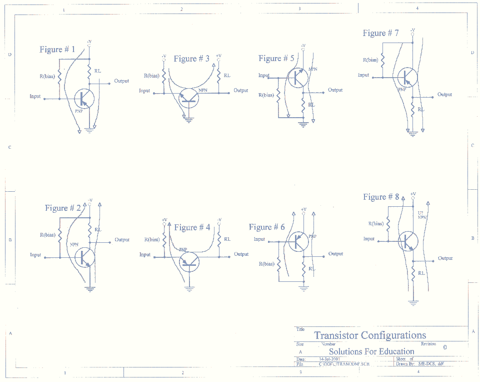
Now look at all 8 of these NPN and PNP Configurations at once: (as a 25Kb gif), (or as a125Kb pdf). I would suggest that you pull up the pdf image and print it out. We can use it to an advantage as we continue our discussions.
All of the textbooks refer to the current relationships in what appears to be rather complicated descriptions. I know that they have their reasons, but it seems to me that if we can establish a major reference point to hinge our thoughts on, the complicated issues will fall into place a great deal easier. In some defense of these complicated issues, the concern of those folks is to establish input vs output relationships with each of these 3 configurations. First of all, it makes no difference whether we use NPN or PNP transistors for our discussions. You should have the full page pdf printed out for this.....
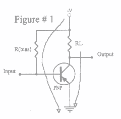
Example #1 (using Figures #1 and #2, the Common Emitter Configuration)
The Input Signal is applied to the Base Circuit, and therefore affects the Base Current. This change in the Base Current affects the Collector Current by a factor of Beta. I.e. if Beta is 120, then the Collector Current will be altered by 120 times the change in the Base Current. An increase in the Base Current from 0 micro-amps to 22 micro-amps will cause a theoretical increase in Collector Current from 0 ma to 2.64 ma. This is simply called the "Current Gain" of the transistor in this configuration. The textbooks refer to this as "The Forward Current Transfer Ratio in the Common Emitter Configuration".
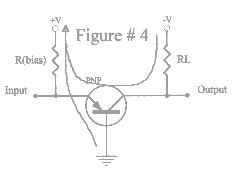
Example #2 (using Figures #3 and #4, the Common Base Configuration)
The Input Signal is applied to the Emitter Circuit, and still affects the Base Current, but because of the involvement of the Emitter Current (which remember contains the Base Current), it becomes a little more complicated. It is worthwhile to note here that since the Emitter Current is composed of the Base Current and the Collector Current, that everyone calls the ratio of Collector Current divided by the Emitter Current "Alpha", which because it is a figure less than "1", it is sometimes expressed as a percentage, or otherwise simply a value like "0.975" (as an example). This simply would mean that if the Emitter Current is 1.4 ma, then the Collector Current would be 1.365 ma. Now, if the Collector Current is 1.365 ma, and the Emitter Current is 1.4 ma, then that must mean that there is .035 ma (or 35 micro-amps) of Base Current in that Emitter Current, along with the Collector Current. If the Collector Current is 1.365 ma, and the Base Current is 0.035 ma, then that means that we have a Beta of 39. The textbooks refer to this as "The Forward Current Transfer Ratio in the Common Base Configuration", where they use the Emitter Current as the Input Current, and the Collector Current as the Output Current.
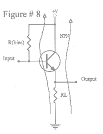
Example #3 (using Figures #7 and #8 (the Common Collector Configuration):
As in Example #1, the Input Signal is applied to the Base Circuit, and therefore affects the Base Current. This change in the Base Current affects the Collector Current by a factor of Beta. I.e. if Beta is 120, then the Collector Current will be altered by 120 times the change in the Base Current. An increase in the Base Current from 0 micro-amps to 22 micro-amps will cause a theoretical increase in Collector Current from 0 ma to 2.64 ma. The difference here is that instead of only looking at the Collector Current, we will look at the composition of the Collector Current and the Base Current, as they exist in the Emitter Circuit. I prefer to consider this as the "Beta +1 Ratio". The textbooks refer to this as "The Forward Current Transfer Ratio in the Common Collector Configuration".